
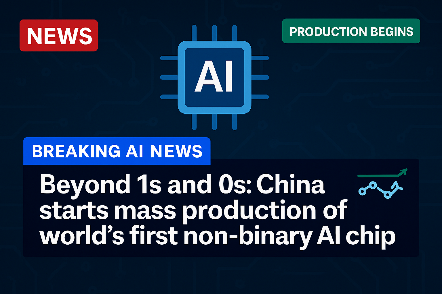
China has initiated the world’s first large-scale application of non-binary AI chips, integrating its proprietary hybrid computing technology into critical sectors including aviation and industrial systems.
Spearheaded by Professor Li Hongge’s team at Beihang University in Beijing, this breakthrough overcomes fundamental barriers in traditional computing by merging binary and stochastic logic, enabling unprecedented fault tolerance and power efficiency in intelligent control applications like touch displays and flight systems while sidestepping US chip restrictions.
Today’s chip technologies face two big challenges: the power wall and the architecture wall, Li told the Beijing-based official newspaper Guangming Daily last month.
The power wall stems from a fundamental contradiction – while binary systems are efficient at carrying information, they consume a large amount of power. The architecture wall is caused by the fact that new non-silicon chips cannot easily communicate with traditional systems based on CMOS or complementary metal-oxide-semiconductors.
Li’s team had been exploring alternatives since 2022. Their breakthrough came with the proposal of a new numerical system – Hybrid Stochastic Number (HSN) – which combines traditional binary numbers with stochastic or probability-based numbers.
Binary logic, the foundation of today’s computing, represents variables using 0s and 1s and relies on precise arithmetic operations. However, large-scale binary computations require extensive hardware resources.
In contrast, probabilistic computing leverages the frequency of “high-level” voltage signals over a fixed time to represent values, significantly reducing hardware consumption. It has already been used in fields like image processing, neural networks and deep learning. But probabilistic computing also suffers from long computation delays due to its frequency-based representation of values.
To solve this, Li’s team introduced hybrid probabilistic logic, which combines the speed of binary computation with the efficiency of stochastic logic.
Based on this concept, the team designed a smart chip for touch and display in 2023 using leading Chinese chipmaker Semiconductor Manufacturing International Corporation’s mature 110-nanometre process technology.
The project results were published in the IEEE Journal of Solid-State Circuits two years ago. The team followed up with a high-efficiency multiplier chip for machine learning, which they fabricated using a standard 28nm CMOS process, according to results published in the Microelectronics Journal in January this year.
According to Guangming Daily, the research marks the first unification of binary, traditional stochastic and hybrid stochastic number systems, offering mathematical representations of each and analysing their characteristics in terms of fault tolerance, interference resistance and energy efficiency.
This provides a strong theoretical foundation for future hybrid probabilistic chip development.
In addition to HSN, the chip incorporates in-memory computing algorithms, which minimise the energy-intensive data shuttling between memory and processors in conventional architectures, thus improving overall efficiency.
It also features a system-on-chip (SoC) design, integrating various types of computing units to handle multiple tasks in parallel, breaking free from the constraints of traditional homogeneous architectures.
The chip is being applied in intelligent control scenarios, including touch recognition, where it filters out noise to detect weak signals and enhance user interaction.
It is also used in instrument displays, where it enables precise, low-power data processing to improve performance and reliability, and flight control systems, where it provides robust computing support for accurate and stable aircraft navigation.
Li told Guangming Daily that the team was working on a dedicated instruction set architecture (ISA) and microarchitecture tailored for hybrid probabilistic computing. They aim to extend the chip’s capabilities to speech and image processing, artificial intelligence large model acceleration, and other complex computing tasks.
“The current chip already achieves on-chip computing latency at the microsecond level, striking a balance between high-performance hardware acceleration and flexible software programmability,” Li said.
Source: https://www.scmp.com/